


Service hotline
+86 18518316054
 Current location : Home page > Resources > Papers > Investigation on graphene and Pt co-modified CdS nanowires with enhanced photocatalytic hydrogen evolution activity under visible light irradiation
Abstract
The hydrogen evolution by photocatalytic water splitting has attracted extensive attention in recent years. Here we report a composite photocatalyst, in which graphene and Pt particles act as cocatalysts to modify CdS nanowires. This composite photocatalyst was prepared by solvothermal method followed by a photoreduction process. The obtained samples were characterized by X-ray powder diffraction, UV-vis diffusion reflectance, scanning and transmission electron microscopy, X-ray photoelectron spectroscopy, photoluminescence and Brunauer-Emmett-Teller specific surface area analysis. The graphene and Pt comodified CdS nanowires gains a high hydrogen evolution rate of 3984 μmol h-1 g-1, which is almost 4 times higher than that of bare CdS nanowires and also higher than the sum of graphene-CdS and Pt-CdS nanowires. The obtained sample also exhibits a good stability. The encouraging results presented here can be attributed to the incorporation of graphene and Pt which show a synergetic effect for hydrogen evolution. This work paves a way to the potential application of CdS nanowires in the energy conversion.
1. Introduction
Hydrogen (H2) evolution from photocatalytic water splitting has attracted enormous attention because it offers a viable and low-cost avenue for solving the energy problems using solar energy [1-4]. To date, various semiconductor photocatalysts have been developed to meet the requirement of H2 evolution or degradation pollutants under light irradiation. Considering the practicability and cost issues, developing efficient, stable and visible-light-driven photocatalysts is still a challenging but significant goals. Cadmium sulfide (CdS), which has a bandgap of ~2.4 eV, has been widely reported and proven to be a suitable candidate for the water splitting into H2 [5-7]. However, CdS alone exhibits a low photocatalytic performance due to the rapid recombination of photo induced electron-hole pairs in the reaction system [8]. In addition, CdS nanoparticles are prone to aggregate leading to a decreasing specific surface area and reactive sites [9]. To solve these two bottlenecks, many attempts have been adopted. Among different strategies, loading CdS on carbon materials, such as graphene, has been proven an ideal approach to enhance the photocatalytic performance of CdS [10-12]. Ye et al. reported that the rate of H2 evolution of graphene-CdS was almost 5 times higher than CdS alone [13], which can be ascribed to the incorporation of graphene. Wu et al. employed a facile method for the preparation of graphene-CdS composite, and the obtained CdS composites are uniformly and densely deposited on the graphene layers with little aggregation [14]. This can be attributed to the properties of graphene. Graphene, a new two-dimensional carbon material, is a promising substrate for photocatalysts, because it has excellent electron conductivity ability and large surface area [15-17]. It can not only act as an excellent carrier acceptor and transfer channel, but also provide large surface area to depress the aggregation.
Another feasible way to improve the photocatalytic H2 yield rate of CdS is the deposition of noble metals, especially platinum (Pt). In general, Pt is considered as the best proton reduction catalyst in the semiconductor photocatalysis and widely used in CdS host system to produce H2 [18]. It is known that the deposition of Pt particles on TiO2 can drastically facilitate the H2 production ability of TiO2 [19]. The same as TiO2, Pt-CdS exhibits a much higher H2 evolution rate [20]. Pt crystallites can trap photo generated electrons and catalyze water splitting to produce H2 [21], especially in the presence of carbon materials [22]. Gao et al. incorporated graphene and Pt crystallites as co-catalysts to improve CdS particles for H2 evolution, and found that the composite possesses 2.5 times higher H2-production rate than that of graphene-CdS [23]. The couple of graphene and Pt into CdS provides a new strategy to obtain high photocatalytic performance in water splitting to produce H2.
It has been known that the morphology and size of semiconductor photocatalysts can significantly influence the photocatalytic performance, because the energetic facet of the photocatalysts can be readily tuned by the morphologies and sized through the quantum confinement effect [24, 25]. According to Iglesias-Juez’s report [26], different morphologies may also affect the exposure of highly-active (polar) surfaces, which is a key parameter to the photocatalytic activity. Recently, a rich variety of photocatalysts with well-defined nanostructures have been widely reported, including nanoparticles [27], nanosheets [28, 29], nanotube [30], nanofibers [31], and nanowires [32] and so on. Nanowires, being one-dimensional structures, may be a promising candidate to obtain an enhanced activity in the photocatalytic reaction. The nanowires with high length-to-diameter ratios always have superior fast and long-lifetime electron transfer capability, leading to a relatively low recombination rate of electron-hole pairs [33]. In this report, we focus on the synthesis of graphene-based Pt/CdS nanowires heterogenous photocatalyst. Compared with traditional nanoparticles, our prepared CdS nanowires also have a greater opportunity to be uniformly anchored on the surface of graphene on geometric consideration. Moreover, [001] facet of CdS has the highest surface energy than other crystal facets [34]. A preferential growth of CdS along the high-energy facet might lead to an enhanced photocatalytic activity. Specifically, the application of the obtained samples in production of H2 and hypothetical mechanism of photocatalytic reaction were also investigated.
2. Experimental
2.1. Preparation of graphene oxide (GO)
Graphite oxide was firstly prepared by a modified Hummers method [35]. 8 g of KMnO4 was added into a mixture of 2 g of natural graphite powder and 100 mL of H2SO4 (98%), and kept stirring in an ice bath for 2 h. The black liquor was transferred into an oil bath at 35 °C and kept for 1 h. Then, 200 mL of water and 30 mL of H2O2 (30%) was added dropwise. The resulted solution was centrifuged and washed with water, and graphene oxide was obtained by freeze-drying finally.
2.2. Preparation of graphene-CdS nanowires
Graphene-CdS nanowires were prepared by a solvothermal method. GO was ultrasonically dispersed in 20 mL of ethylenediamine (EDA). Then 5 g of Cd(NO3)2 •4H2O and 3.7 g of thiourea was added into the GO suspension under stirring. The homogeneous solution was transferred into a 50 mL Teflon-lined autoclave which was then filled with EDA to 80% of the capacity. Then the autoclave was held at 160 ºC for 48 h. After that, the precipitates were collected by centrifugation, and washed by water for several times to remove the residue of EDA. The final product was dried at 80 ºC under vacuum, which had a ratio of graphene/CdS =1%. At the same time, bare CdS nanowires were prepared in the absence of GO. The samples were defined as CdS NWs and G-CdS NWs, respectively. For comparison, the graphene-CdS nanoparticles were prepared by a hydrothermal method reported in our previous paper [12].
2.3. Preparation of graphene-Pt-CdS nanowires
To deposite Pt crystals on CdS NWs, photoreduction method was employed. 1 g of the obtained CdS or graphene-CdS samples were dispersed in 80 mL of acetic acid solution (0.25 M) containing 1 mL of H2PtCl6 solution (0.05 M) and 0.5 g of Cd(Ac)2•2H2O. The mixture was degassed to remove the dissolved oxygen and irradiated by a 300 W Xe lamp for 30 min. The obtained products were collected, washed and dried at 80 ºC under vacuum, which were named as Pt-CdS NWs and GP-CdS NWs, respectively. The graphene-Pt comodified CdS nanoparticle sample was prepared by similar method just replace graphen-CdS nanowires with graphene-CdS nanoparticles.
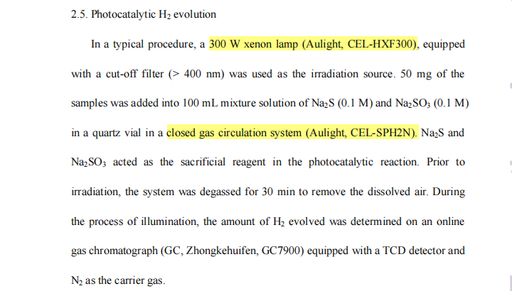
2.5. Photocatalytic H2 evolution
In a typical procedure, a 300 W xenon lamp (Aulight, CEL-HXF300), equipped with a cut-off filter (> 400 nm) was used as the irradiation source. 50 mg of the samples was added into 100 mL mixture solution of Na2S (0.1 M) and Na2SO3 (0.1 M) in a quartz vial in a closed gas circulation system (Aulight, CEL-SPH2N). Na2S and Na2SO3 acted as the sacrificial reagent in the photocatalytic reaction. Prior to irradiation, the system was degassed for 30 min to remove the dissolved air. During the process of illumination, the amount of H2 evolved was determined on an online gas chromatograph (GC, Zhongkehuifen, GC7900) equipped with a TCD detector and N2 as the carrier gas.
3. Results and discussion
3.1. Characterization
A series of samples were studied by XRD to identify their phase structure, and the results are shown in Fig. 1. As can be seen, all the samples exhibit similar pattern, which can be assigned to the well-defined hexagonal phase of CdS (JCPDS 41-1049). It should be noted that the XRD pattern of CdS NWs has no change after the introduction of graphene and Pt, implying that the presence of graphene and Pt did not alter the crystallite morphology and nanowire size. Unfortunately, no typical diffraction peaks of graphene and Pt are observed in the patterns, which may be ascribed to their low content. The morphologies of the samples were firstly observed by SEM, as shown in Fig. 2. CdS NWs sample shows the one-dimensional morphology of characteristic nanowires with a length of ca. 0.5~ 2 μm and an average diameter of ca. 40~ 50 nm in Fig. 2(A~B). It indicates that a good quantity of CdS NWs with high uniform dimensions can be obtained by our solvothermal method. For G-CdS NWs composite, it can be seen CdS NWs are promiscuously anchoring on the graphene nanosheets, which exhibit large surface area with some wave-like wrinkles on the edge (Fig. 2(C)). As can be seen, the graphene nanosheets and CdS NWs have been successfully integrated. Fig. 2(D) shows SEM image of Pt-CdS NWs, in which some tiny Pt particles with average size of ca. 20 nm are dispersing on the surface of CdS NWs. In Fig. 2(E), GP-CdS NWs shows a similar image with G-CdS NWs, except for some small noble metal Pt crystals. There is essentially no change to the morphologies of CdS NWs during the introduction of graphene nanosheets and tiny Pt particles. For GP-CdS NWs, the hybridization between CdS NWs and Pt was further confirmed by EDX elemental mapping analysis. Fig. 3 shows the typical elemental mapping images of Cd, S and Pt, respectively. It is very clear that the Cd, S and Pt elements are uniformly distributed in the composite photocatalysts, providing strong evidence for the homogeneous formation of heterojunctions. TEM was carried out to provide further insight into the microscopic morphologies and structure of the as-obtained GP-CdS NWs. As can be seen from TEM images in Fig. 4(A), the curly, transparent and sheet-like structure is clearly observed for two-dimensional graphene. The crumpled graphene sheets have an adequate interfacial contact with one-dimensional CdS NWs. Some CdS NWs are even encapsulated by graphene nanosheets. The average size of Pt particles is approximately 20 nm in diameter, which is in agreement with the observations from SEM. The Pt spheres are anchoring on the surface of CdS NWs, and also wrapped by graphene. It indicates the good interfacial contact formed among graphene, Pt and CdS NWs. The HRTEM image displayed in Fig. 4(B) shows that the lattice fringe is 0.335 nm, consistent with the crystallographic plane (002) of hexagonal wurtzite-structured CdS (JCPDS 41-1049). It reveals that the CdS NWs grew preferentially along the c-axis [001] orientation [36, 37]. The optical properties of the as-prepared samples were investigated by the UV-vis DRS. It can be seen from Fig. 5(A) that, the incorporation of graphene and Pt particles can significantly enhance the absorbance in the visible light region as compared to pure CdS NWs, especially when Pt involved. From previous reports, the noble metal Pt loading on the photocatalysts can absorb large amounts of visible light [38, 39], especially in the region of 400~ 500 nm. In addition, GP-CdS NWs exhibited higher light absorbance than G-CdS NWs and Pt-CdS NWs, which may favor the photocatalytic performance. Plots obtained from the transformation of DRS results based on the Kubelka-Munk function versus photon energy are shown in Fig. 5(B). The estimated band gap value of CdS NWs are about 2.36 eV, which was consistent with the previous articles [8, 33, 36]. No significant changes can be observed in the band gap values for all the samples, suggesting that the introduction of graphene and Pt have negligible effect on the band gap of CdS NWs.
The representative XPS spectra of the as-synthesized GP-CdS NWs are shown in Fig. 6. The survey XPS spectrum (Fig. 6) shows the presence of Cd, S and C along with Pt in the following binding energy ranges: Cd 3d region (397~ 420 eV), S 2p (156~ 170 eV), C 1s (276~ 296 eV) and Pt 4f (69~ 82 eV). The Cd 3d core level could be satisfactorily fit to two peaks of Cd 3d5/2 at 405.07 eV and Cd 3d3/2 at 411.84 eV, indicating that cadmium was in Cd2+ state [40]. In the case of the XPS spectrum of S 2p, two peaks have been well fitted, namely S 2p3/2 (161.42 eV) and S 2p1/2 (162.58 eV), which can be assigned to S2- [13] as expected. As shown, the XPS spectrum of C 1s can be deconvoluted into three smaller peaks, which was ascribed to the following functional groups: sp2 bonded carbon (C-C, 284.72 eV), epoxy/hydroxyls (C-O, 285.68 eV) and carbonyls (C=O, 286.95 eV) [41]. In comparison to the GO spectrum reported previously [42], the intensities of peaks for C-O and C=O are much weaker, indicating that most of these oxygen-containing functional groups were removed in the solvothermal reaction, thus graphene has been obtained from GO. The binding energies of Pt at 72.45 eV and 75.77 eV were ascribed to Pt 4f7/2 and Pt 4f5/2, respectively, which disclosed that Pt existed as a metallic form Pt0 in the sample [43, 44]. The detailed information of experimental XPS assignments is listed in Table 1 and Table 2, together with the theoretical energies. It can be noted that the experimental energies have shifted in comparison with the theoretical values. However, the difference values and ratios of area between the two characteristic peaks of Cd 3d, S 2p and Pt 4f were approximately in agreement with the theory. For C 1s, the peak positions also shifted, which may be attributed to the random error and physicochemical property of the sample. The fractions of different functional groups showed that C-C was the dominate group in C 1s, confirming that graphene oxide was reduced.
PL analysis has been widely used to investigate the lifetime of electron-hole pairs in semiconductor materials. When the recombination of electron-hole pairs occurs, photons are emitted, leading to the photoluminescence. In other words, the lower recombination rate, the weaker PL signal intensity is. Fig. 7 illustrates the PL spectra of the as-prepared samples excited at 360 nm. The PL spectrum of CdS NWs shows a strong emission peak at 535 nm, which is attributed to the well-known surface vacancies belongs to trap emission of CdS [45]. Obviously, compared with CdS NWs, the intensity of PL signal for the G-CdS NWs and Pt-CdS NWs are lower. Additionally, the PL intensity for GP-CdS NWs is significantly quenched, suggesting that GP-CdS NWs has the lowest recombination rate of electron-hole pairs.
3.2. Photocatalytic behaviors for H2 evolution
To investigate the photocatalytic performance of the synthesized catalysts, the H2 production activity was evaluated under visible light irradiation. In control experiments, no appreciable H2 yielded was detected in the absence of either photocatalyst or light irradiation (data not shown here). Time-dependent GC spectra for H2 evolution over GP-CdS NWs are given in Fig. 8(A). In the spectrum, the peak area of H2 keeps progressive increase with the extending of irradiation time. Fig. 8(B) shows the comparison of visible-light photocatalytic H2-production amount of different NWs samples within 5 h. All photocatalysts show nearly constant rates of photogeneration of H2 in 5 h. In addition, the average rates of H2-production over different samples are shown in Fig. 8(C). It can be clearly seen that graphene and Pt exhibit significant influence on the photocatalytic activity. The pure CdS NWs generated 254.84 μmol of H2, and its rate was 1022 μmol h-1 g -1. The rate increased with the addition of either graphene or Pt particles to 1344 and 1933 μmol h-1 g -1, respectively. Synergistic effects between graphene and Pt promoted the H2 yield of CdS NWs to 3984 μmol h-1 g -1, which is obviously greater than the sum of that of G-CdS and Pt-CdS NWs under the same experimental conditions. It also shows higher than the rate by graphene-Pt co-modified CdS nanoparticles which is 1924 μmol h-1 g-1. The GP-CdS NWs possessed higher visible-light-induced H2-production ability than most photocatalysts reported in other literatures, such as TiO2 (68 μmol h-1 g -1) [46], G-TiO2 (740 μmol h-1 g -1) [46], Pt-TiO2 (2915 μmol h-1 g -1) [19], G-ZnxCd1-xS (1824 μmol h-1 g -1) [42].
For G-CdS NWs, it provided an enhanced H2-production rate than pristine CdS NWs. In general, it can be attributed to the superb electron-conductivity of graphene. The presence of graphene can efficiently decrease the likelihood of the recombination of photo induced electron-holes pairs over CdS NWs, thus leading to a prolonged lifetime of charges. This is because graphene has an excellent capability of capturing, collecting and transferring electrons [47, 48]. The efficient separation of electron-hole pairs is beneficial for the enhanced photocatalytic H2-production activity over the bare CdS NWs. It should be noted that the H2 evolution rate of Pt-CdS NWs was almost double of that of naked CdS NWs alone, as Pt is an efficient cocatalyst for photocatalytic H2 evolution. Noble metal, Pt particle here, has a Fermi level lower than the conduction band of most semiconductors. Thus Pt can attract and collect free electrons in the photocatalytic reaction, eliminating the availability of extra charges for recombination with holes and leading to increased electrons available for H2 production.
Another factor influencing the photocatalytic reaction is the optical properties of the photocatalysts. Depending on the UV-vis DRS analysis, it can be seen that the introduction of graphene and Pt have a significant effect on the absorption intensity in the visible light region ranging from 400~ 800 nm. When graphene and Pt were both involved, the GP-CdS NWs exhibited the highest light harvesting property among the as-prepared samples. The enhanced absorption may have a benefit influence on the photoactivity, because it could offer higher light intensity for the semiconductor CdS NWs. Therefore, graphene and Pt particles can act as photosensitizer chemically bonded with CdS NWs.
Besides the two aspects mentioned above, the surface area may also affect the photocatalytic performance. Larger surface area can provide more active sites for the semiconductors, thus accelerating the reaction and resulting into a higher photocatalytic activity. Measurement of BET specific surface area obtains 19.54, 21.31, 20.50, 19.55 m2g -1 for CdS, G-CdS, Pt-CdS and GP-CdS NWs, respectively. No marked differences in surface area was found when graphene and Pt was introduced, which may caused by the low content of cocatalysts. Therefore, the effect of surface area on the photoactivity can be ignored in the present study.
According to previous reports, the graphene nanosheets in our study probably involves defects occurred during the chemical reduction process from exfoliated graphite oxide sheets [49]. From the TEM images, some Pt nanoparticles are wrapped by graphene nanosheets. The presence of these extremely tiny Pt particles indicated a strong and close interaction between graphene nanosheets and Pt crystals. The interaction between graphene and Pt may induce some modulation within the electronic structure of Pt. According to Okamoto’s research [50], the interaction between Pt and graphene with many carbon vacancies can be enhanced than that on defect-free graphene, leading to an increased stability of Pt. This result indicated that defective graphene can act as a carbon support to modify catalytic properties of Pt-involved catalysts. Yoo et al. [51] have also reported that graphene-based Pt exhibit unusually high electrocatalytic activity because of the existence of vacancies within graphene. Thus it can be concluded that defective graphene in our study can perfect the specific electronic structure of Pt. The synergistic effects between Pt and defective graphene sheets may be responsible for the highly enhanced H2-productin activity of GP-CdS NWs in comparison with G-CdS and Pt-CdS NWs. The synergy index can be quantified from the H2 production rate using a simple equation [52] as following:
Synergy index = RGP / (RG + RPt) Eq(1)
...
Beijing China Education Au-light Co., Ltd.
Room 401, Fengtai Science and technology innovation center, No. 7 Kexing Road, Fengtai District, Beijing
+86 18518316054
eric@aulight.com;info@aulight.com

Scan and pay attention to us